
PCB Milling and Printing
Project Summary
This document will give an outline to PCB milling for two-sided, copper PCB plates and to printing PCBs from blanks. The Voltera is used for printing blanks and drilling for both processes. The Carvey is used for milling traces into copper-plated board.
Project Details
- Board Design
- If designing with Fritzing…
- Open Fritzing > make breadboard > check circuit-diagram > lay out on PCB
- Set board-type (1 or 2 sided, in info panel on bottom-right)
- Autoroute traces (bottom bar)
- Check design calculations (Routing > Design Rules Check)
- Export as an Extended Gerber for the Voltera and as an SVG for the Carvey (bottom bar)
- If designing in Eagle..
- Open Eagle > make circuit-diagram > lay out PCB
- Set board type (1 – multi-layered) by drawing in different layers
- Formatting
- If power-planes are desired, they can be added by drawing a “polygon” around the desired region > name it the same as desired signal> rats-nest > make sure the pad is connected to the proper signal by clicking the signal with “Name” tool (on the left)
- Distance between paths and power-planes can be changed with a right-click on the polygon > properties > isolation
- To remove power-planes use “RIPUP @;” in the command line
- If you want to move component names without moving the components, use “SMASH”
- “Design-Rules-Check” on the left-hand side provides and in-depth menu to change pad and trace widths and sizes (among other things)
- Pad size can also be individually changed with the “Info” > diameter or can be changed in the component library. WARNING: changes made in component libraries will not auto-reset
- If designing with Fritzing…
- Autoroute traces (left-hand bar)
- Check design and electronics calculations (left-hand bar)
- View what the board will eventually look like with “Manufacturing” (right-hand side)
- File > CAM Processor > preview board > go to drill document settings > advanced > set integer to 2 and decimal to 4 (imperial standard)
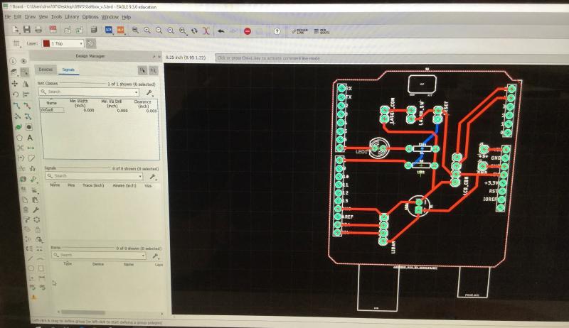
Figure 1 - The Eagle PCB development screen showing where the main tools can be found. Side-bar: move, name, info, polygon, ratsnest, design-rule-check, electronics-rules-check, route, autoroute, group. Top-bar: CAM Processor, view, save, layer
- Board Manufacturing
- If cutting with Carvey…
- In Eagle, move board more than 1in up (as to not run into the clamp, groups > ctrl + right-click + “Move”) > center board on final workpiece (for 2-sided board) > CAM Processor > export Gerber file
- If cutting with Carvey…
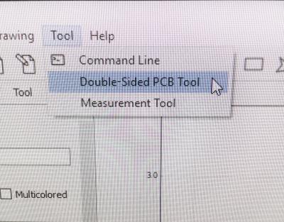
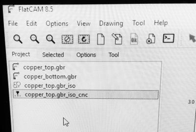
| Figure 2 - Top: location of double-sided PCB tool. Bottom: an example of the different files needed to be generated to develop gcode. |
- Open FlatCAM > load Gerbers > Tool (top bar) > Double-sided PCB Tool > select bottom Gerber file > export mirror > select Gerber files under project tab > adjust relevant settings: tool-size (~.02in), isolation passes (2 an up normally), combine passes (check) > generate geometry > set CAM parameters (.iso file) > cut-depth (-.01) > export as g-code
- Now open Easel > load gcode file > load tool > clamp piece > adjust tool size (same as FlatCAM designation), workpiece dimensions, and feed speed (30 in/min) > follow print dialogue (feed-speed can be increased and decreased 100% after carving begins
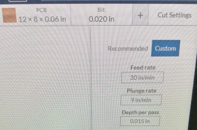
Figure 3 - General Carvey tooling parameters for PCB milling.
- If printing in Voltera…
- Open Voltera > load file > simple print > follow print dialogue (for board with preexisting components use the “aligned” option)
- If drilling and printing in Voltera…
- Select ink > upload Gerber file for paths > load hole-map> follow print-dialogue
- If drilling with Carvey and printing in Voltera
- Open hole-map SVG in Easel > mill holes (fill not outline) > open trace- and hole-map Gerbers in Voltera > aligned print > follow print dialogue
Remote Assets